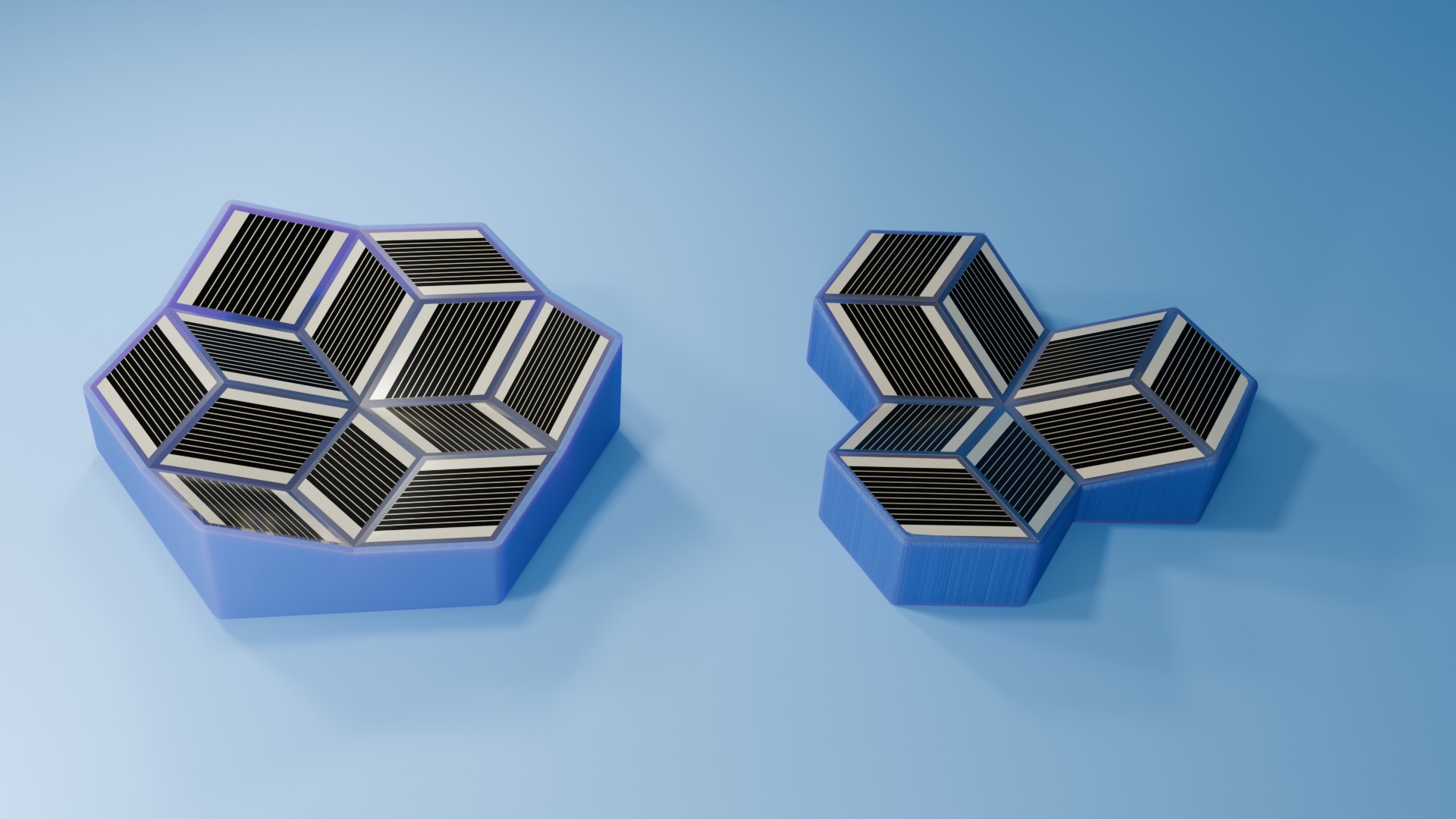
Perovskite Solar Module — Where Physics Meets Form
A lab-stage perovskite photovoltaic prototype becomes a product people want to buy: hexagonal modularity, crystal-derived aesthetics, and scalability without losing visual coherence.
Context: what perovskite is and why it matters
Perovskite is a class of crystalline materials with the general formula ABX₃. In photovoltaics, it's not just a new material — it's a potential revolution in solar cell manufacturing. Conventional monocrystalline silicon requires complex high-temperature production. Perovskite photovoltaic cells can be deposited from solution at low temperature — printing instead of crystal growth.
Lab-stage perovskite cells have exceeded 25% efficiency — comparable to the best silicon panels. The problem: a lab sample and a commercial product are different things not only technically, but visually. A perovskite prototype looks like a prototype: functional, but not something investors or end customers would want to buy.
The hexagonal form was not invented — it was read from the material. Perovskite's polycrystalline structure under microscopy shows grain boundaries with characteristic six-fold symmetry. The design literally grows from the physics of the material.
Brief: from prototype to product
The task was to turn a laboratory sample into an object presentable to investors, exhibitable at trade shows, and pitchable to potential B2B clients. Key requirements: aesthetics should reflect the material's nature, the system must scale for different applications, one element is the foundation of the entire product line.
Concept: hexagonal modularity
Why hexagon
The hexagonal module form is not an aesthetic choice. A regular hexagon provides maximum area coverage in tessellation without gaps — like a honeycomb. When assembling an array from multiple modules, there are no unused gaps. Fill factor: 100%.
Additionally, the hexagon is the only regular polygon after the square that maintains symmetry at scale. A 60° rotation produces an equivalent configuration — critical for modular systems where element orientation is variable.
Assembly configurations
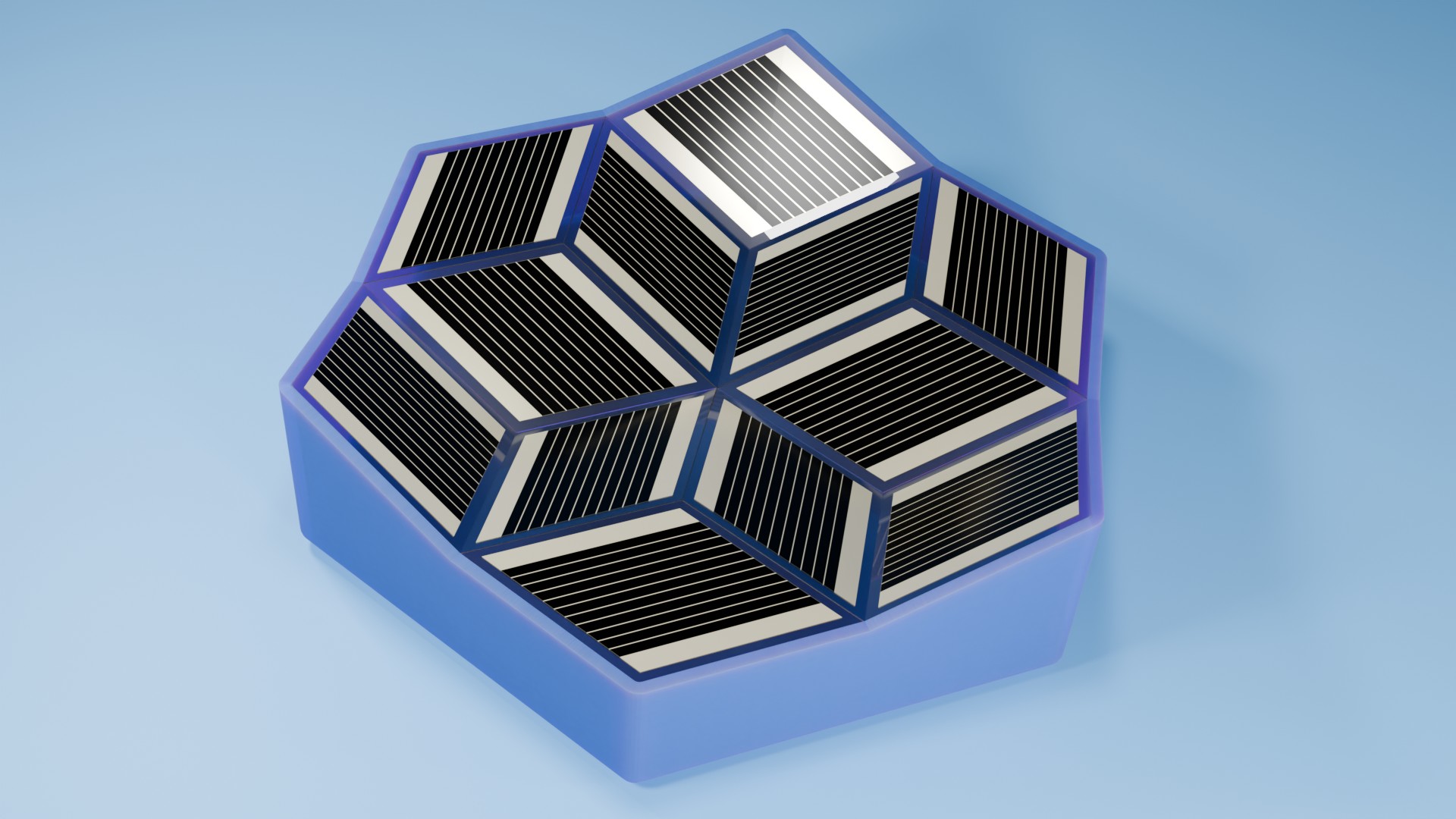
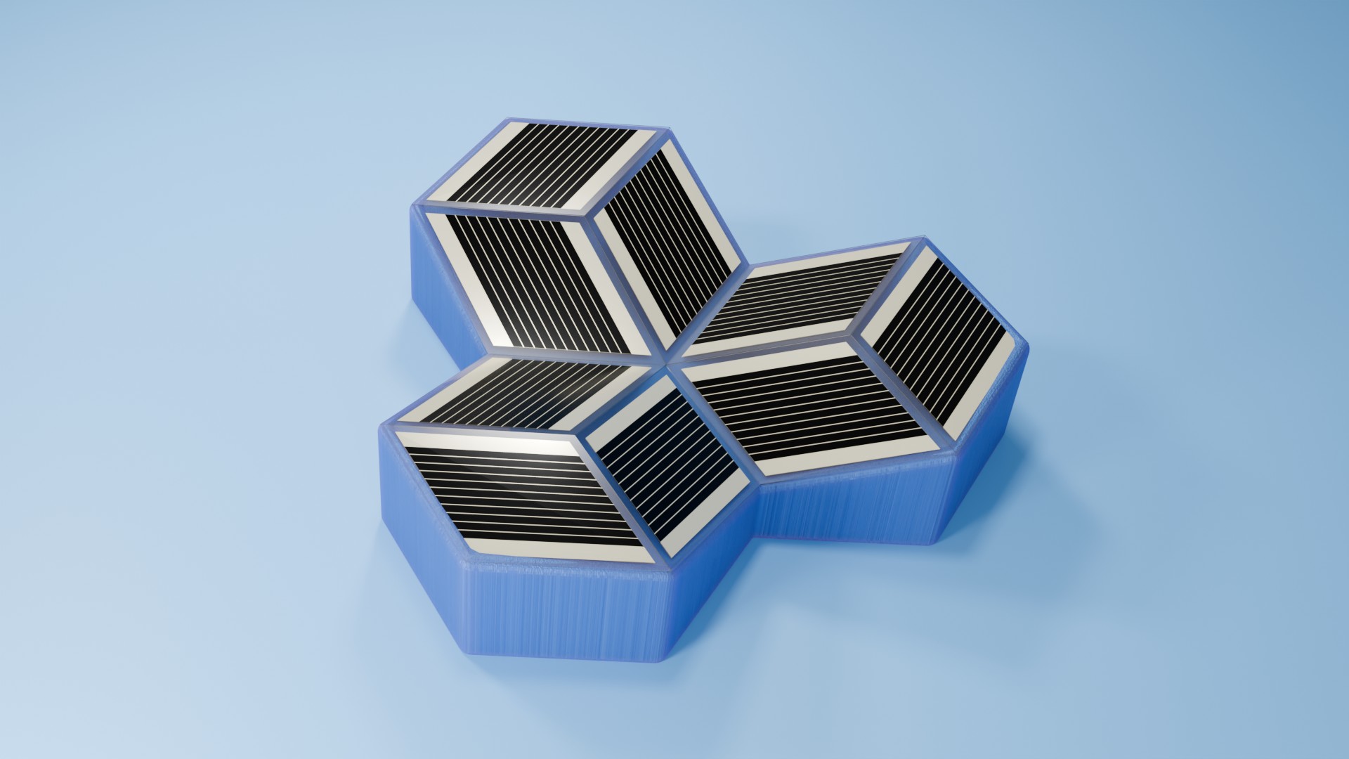
From a single base hexagonal element, several configurations were developed: a compact "flower" of seven elements (one central, six surrounding), a cross-shaped configuration of four, a linear strip. Each configuration serves different purposes — the flower for compact autonomous installations, the strip for facade integration.
The element connection mechanism is designed so that joints read as design features rather than technical compromises. Element frames meet in a shared aluminium profile that simultaneously serves as structural support and cable channel.
Colour scheme
The colour solution mimics the physical properties of perovskite. Depending on composition and layer thickness, a perovskite film shifts colour from deep brown to yellow-green. The dark-to-light gradient within a module references this property — while creating visual depth that mimics the crystal lattice.
Process: from crystal to CAD
Work began with studying the material: microphotographs of perovskite films, crystallography of the ABX₃ structure, existing commercial solar panel formats. This is necessary so the form isn't arbitrary — it needs a rationale that can be explained to an investor.
The first sketching phase transformed crystalline symmetry into flat module geometry. The second phase worked out the connection mechanism: how hexagons join without gaps, how cable routing is concealed, how thermal expansion is accommodated across operating temperature ranges. The CAD model was built for realistic manufacturing constraints: the frame profile is a standard aluminium extrusion section, not custom — reducing first-run production costs without aesthetic compromise.
Result
A design concept ready for production handoff: 3D renders, colour scheme, modularity logic. The product now looks as convincing as it works. The design solves a concrete business problem: translating a technological breakthrough into a visually legible product for investors and B2B clients.
What this means for deep tech companies
There's a persistent illusion at early-stage companies: design can be added later, once the technology is ready. Practice shows the opposite. Investors make decisions in pitch sessions where 10 minutes is the maximum. If the product looks like lab equipment rather than something you'd want to fund, chances of the next round fall significantly. The perovskite module shows how design creates value at zero commercialisation stage: the technology exists, the product doesn't yet — but there's a visual story already being told.